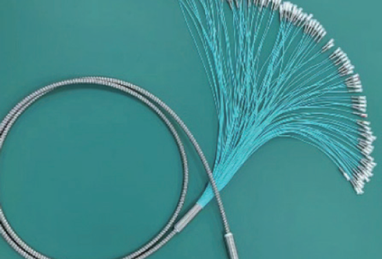
Fiber Arrays in PCB Board Lithography
In the ever – changing landscape of electronic manufacturing, PCB (Printed Circuit Board) lithography stands as a cornerstone of progress. Among the numerous innovations in this field, fiber arrays have emerged as a game – changer, playing a pivotal role in enhancing the precision and efficiency of PCB manufacturing, which is indispensable for modern electronic devices.
Understanding Fiber Arrays
Fiber arrays are essentially bundles of optical fibers engineered to efficiently transmit light across a wide range of applications. In the context of PCB board lithography, their significance lies in their ability to ensure uniform light distribution across the PCB surface during the exposure phase. This uniform light distribution is the linchpin for creating accurate patterns on the photoresist material, which, in turn, forms the basis of the circuitry.
Applications in PCB Lithography
Laser Cutting
The integration of fiber arrays has revolutionized laser cutting techniques in PCB manufacturing. By leveraging precise laser beams guided through fiber optic systems, manufacturers can now create highly intricate designs. Whether it’s a hexagon, circle, or rectangle pattern, the level of control offered enables the production of detailed circuitry essential for high – performance electronics. This precision not only enhances the functionality of the PCBs but also opens up new possibilities for miniaturization and complex circuit design.
UV Optical Fiber Technology
The potential of UV optical fibers in PCB lithography is being increasingly tapped into. These fibers are capable of delivering UV light for exposure processes, resulting in faster curing times and improved pattern alignment accuracy. The ability to manipulate light at the microscopic level gives manufacturers a competitive edge in achieving high – precision results. This is particularly crucial as the demand for smaller and more powerful electronic devices continues to grow, requiring ever – more accurate PCB manufacturing processes.
Versatile Array Configurations
One of the key advantages of fiber arrays is their versatility in configuration. They can be customized into various shapes, including hexagonal, circular, or rectangular arrangements. This adaptability allows manufacturers to optimize their lithography processes according to specific design requirements. For example, a hexagonal array might be more suitable for a particular circuit layout, while a circular one could be better for another. This flexibility not only enhances the efficiency of the production process but also enables the creation of unique and optimized PCB designs.
Quality Control and Inspection
After the lithography process, ensuring the accuracy of the PCB is of utmost importance. Fiber arrays play a vital role in inspection systems, offering high – resolution imaging capabilities. These capabilities enable the detection of even the smallest defects, ensuring the integrity of the final product. By using fiber arrays for quality control, manufacturers can reduce the number of defective products, saving both time and resources in the long run.
Our company has taken this technology a step further by combining unique dense row technology with a nano – scale polishing process. This combination maximizes the transmission efficiency of bundled optical fibers. Additionally, we offer customized connectors to meet the diverse needs of our customers, enabling the on – demand transmission of light energy with multiple inlets and multiple outlets. This makes our customers’ optical systems more flexible, convenient, stable, and reliable, providing them with a competitive edge in the market.
